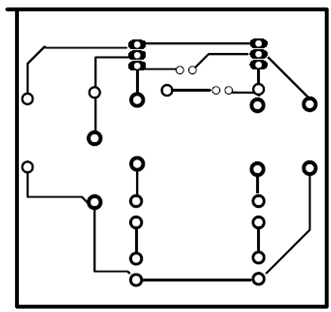
PCB design for 4LED Flasher
Circuit schematic of 4 LED flasher
Hard to find PCB design for the Flasher circuit using 4 LEDs are given below. One can easily and quickly etch this design on a small copper clad board and prepare a PCB of your own. It is economical and cost effective to prepare your own PCB of this type. Normally these type of PCBs are hard to find in the electronics mart. Hence the design is given for your use.
This component layout schematic will help you to easily locate the component placement on the PCB. It is easy to identify the components of the circuit and its location
 |
| component layout |
Circuit Schematic
Though the circuit has been fully described in the previous post , for ready reference the same is given here to facilitate to understand the set up and design.
 |
| 4 KED flasher circuit schematic |


Components are attached to PCBs using a number of different soldering methods. Large scale production is usually done with machine placement and most likely reflow ovens. Very tiny components may be attached by highly skilled professionals with the help of a microscope and precision tools. PCB production
ReplyDeleteThe tag antenna is deposited or printed on the substrate, and the IC is then attached to this antenna. A substrate is usually made from flexible material such as thin plastic, but it may also be made from rigid material. Most passive tags use substrates made from flexible material with a thickness of 100 to 200 nm. If you want to know more, Please check out here - rfid label suppliers
ReplyDelete